Laser Micromachining Technology

The Hi-Nano team boasts over two decades of focused development in laser micromachining technologies, enabling industry advancement. Our expertise shines in solving intricate micron-level challenges, particularly with ultra-hard materials like diamonds, sapphire, silicon carbide , lithium niobate, optical glass and beyond. Whether it's tailored machining or cutting-edge system production, rely on Hi-Nano for unmatched proficiency. Join us in this journey now!

Advanced AR Lens Cutting

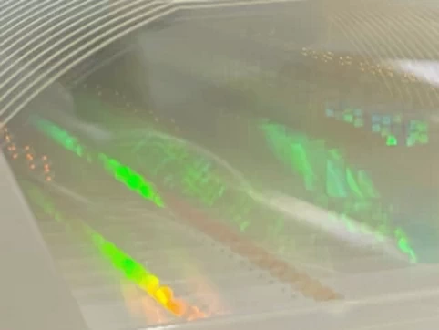
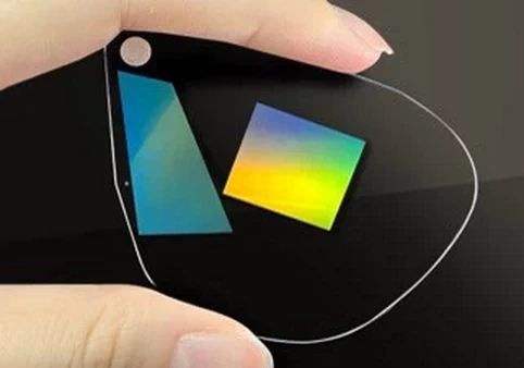
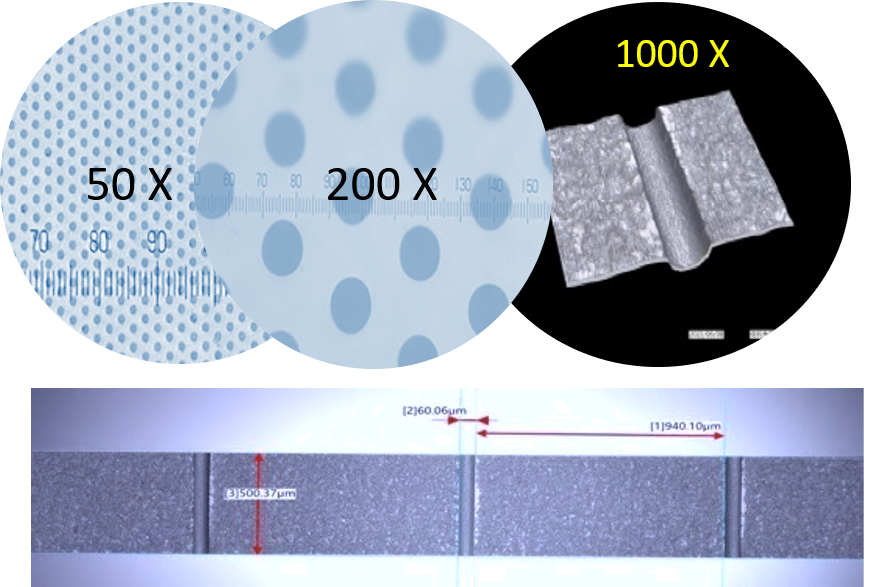
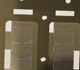
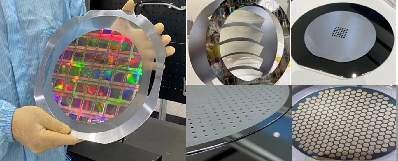
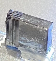
When working with AR /VR wafers that incorporate nano-scale optical gratings and waveguides, it is crucial to exercise caution during the processing phase.

These wafers are composed of specialized materials, requiring unique methods for dicing compared to the more common optical glass dicing. Hi-Nano boasts a field-proven technology with extensive experience in effectively managing these challenges.

Features:

  • Achieve micron-level precision with utmost accuracy.
  • Employ a non-contact process to ensure minimal particle formation and maintain cleanliness.
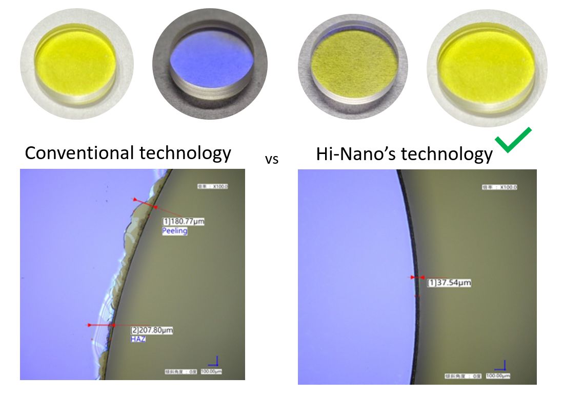
  • Experience negligible heat-affected zone (HAZ) for pristine results.
  • Minimize chipping and micro cracks during the cutting process.

Applications:

  • Optical wafer dicing for precise manufacturing in the optics industry.
  • Cutting AR and VR glasses with utmost precision.
  • MEMS wafer dicing for micro-electromechanical systems.
  • Cutting coated lenses with exceptional accuracy.
  • Laminated optics cutting for seamless integration of optical components.
  • Optical sensor cutting for intricate sensor devices.

Embrace the precision and versatility of our Nanostructured Glass Wafer Cutting
for cutting-edge solutions in various industries.

Glass cutting and hole drilling

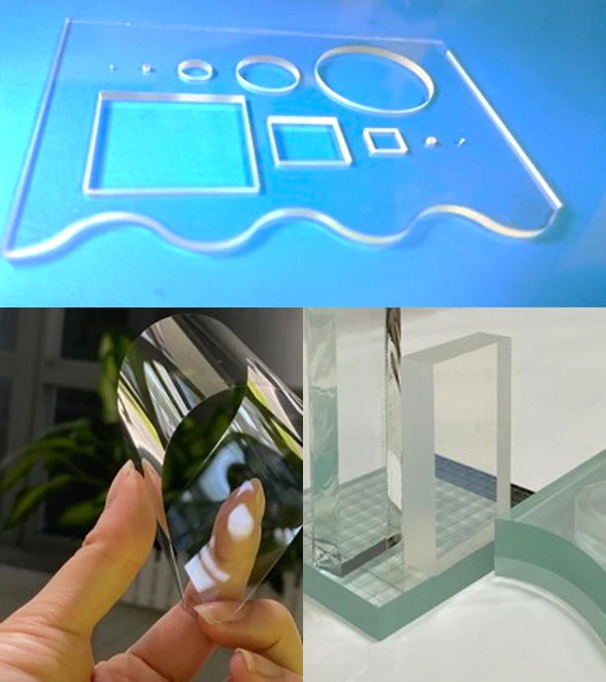
Hi-Nano has developed an array of advanced technologies for processing various types of glass used in industries like semiconductors, optoelectronics, AR/VR, FPD, automotive, drones, and medical devices.

Our expertise covers a wide thickness range from 10 micrometers to 10 millimeters, encompassing tasks like cutting, micro hole drilling, engraving, marking, welding, and polishing.”

Features:

  • Capable of cutting both straight lines and free shapes with precision.
  • Accommodates a wide range of glass thicknesses, from ultra-thin and bendable to ultra-thick glass.
  • Enables cutting and drilling of various optical glass types with exceptional accuracy.
  • Delivers high cutting quality for coated lenses, ensuring superior results.

Applications:

  • Cover glass and view windows for electronic devices and displays.
  • Optical sensors, providing accurate and reliable sensing capabilities.
  • Glass substrates for diverse electronic and optical applications.
  • Car mirrors, ensuring safety and clarity for drivers.
  • Optical lenses, crafting lenses with precision and efficiency.
  • Glass components for various industrial and consumer products.
  • Laminated glass for enhanced durability and functionality in specialized applications.

Unlock the potential of our versatile technology, empowering your projects with precision and efficiency across a myriad of applications.

TGV (Through Glass Vias) and Glass Core

By harnessing the power of ultra-short pulse lasers, we can modify the interior of a glass wafer. Subsequent wet processes etch away the modified sections, resulting in the creation of vertical through holes or intricate horizontal channels. This revolutionary approach has ushered in a new era of semiconductor 3D packaging possibilities and enabled the development of high-frequency, low-loss glass substrates for advanced communication and cutting-edge medical devices.

Features:

  • Holes available in straight or hourglass shapes.
  • High aspect ratio capabilities, extending up to 1:20.
  • Achievable minimum micro hole size, with diameters as small as 20 micrometers.
  • Remarkable precision levels for consistent results.
  • Cost-effective manufacturing process.

Samples: Cross-Sectional View and Top View of TGV

Material : Optical Glass, Thickness = 200um
Hole dia. : > 25 um
Aspect Ratio : Max. 1:20

TGV and glass core technologies are key enablers in the development of advanced communication systems, AI devices, and semiconductor packaging. Their applications in mmWave technology contribute to the evolution of high-frequency communication and connectivity in the realms of 5G, 6G, LEO communications, and beyond. Additionally, their role in heat spreading enhances the overall performance and reliability of electronic components.

TGV and Glass Core Applications:

TGV (Through Glass Vias): TGV technology, with its ability to create electrical connections through glass substrates, contributes significantly to various applications:
  • 5G and 6G Communications:In high-frequency communication systems such as 5G and upcoming 6G networks, TGVs are crucial for enabling miniaturization, reducing signal loss, and optimizing the performance of RF (Radio-Frequency) devices that operate at millimeter-wave frequencies.
  • LEO Communications:In Low Earth Orbit satellite systems, TGVs can be used in RF components and antennas for high-frequency communication, ensuring reliable connectivity for data transmission.
  • AI Devices:TGVs play a crucial role in AI-related devices by providing compact and efficient electrical connections within components like sensors, accelerometers, and processors. This contributes to the miniaturization and improved performance of AI hardware..
  • Advanced IC Packaging:In advanced IC packaging, TGV technology is harnessed to create compact and high-performance semiconductor packages. This is particularly crucial in applications where space constraints and thermal management are critical.

These are just a few examples; in fact, numerous additional applications are currently in development.

Coated Lens Cutting

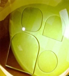
Optical lenses for various applications often feature multiple layers of coatings like HR (High Reflect) and AR (Anti-Reflect) on both sides. Traditional methods, whether mechanical or laser dicing, frequently lead to issues such as peeling, chipping, and HAZ problems.

Hi-Nano introduces groundbreaking laser dicing technology, significantly elevating dicing quality. Our approach delivers consistently flawless cuts, addressing the challenges tied to coated layers.

Features:

  • Superior Cutting Quality.
  • Absence of peeling.
  • Minimal chipping and HAZ.
  • Zero contaminations.
  • No scratches.

Applications:

  • Miniaturized cameras and sensors for smartphones and wearables.
  • Endoscopes and minimally invasive medical devices for internal imaging and diagnostics.
  • Micro optics for coupling light signals in compact optical communication devices.
  • Miniature Lidar systems for robotics, drones, and autonomous vehicles.
  • Optical sensors for fingerprint recognition and gesture control.
  • Compact vision systems.
  • Smart glasses and AR devices.
  • Mini. cameras and sensors for (UAVs) and drones.

Sintered SiC Machining

Sintered Silicon Carbide (SiC) is a dense, durable ceramic vital for semiconductor equipment. Yet, conventional machining is slow due to its hardness. Hi-Nano’s advanced laser technology makes SiC machining faster, easier, and wear-free, resulting in significant cost savings.

Features:

  • Non-Contact Processing
  • Micro-Machining Capabilities
  • Zero Tool Wear
  • Precision and Accuracy
  • Minimal Heat Affected Zone (HAZ)
  • Reduced Material Waste
  • Reduced Processing Time.
  • Significantly lower manufacturing costs.

Applications:

  • Employed as wafer chucks, susceptors, and carriers in the Chemical Vapor Deposition (CVD) and epitaxy processes for semiconductor fabrication equipment.
  • Utilized as electrodes and components within dry etching equipment’s chambers and more.
  • Integrated into aircraft brake disks to enhance performance.
  • Utilized for mechanical components across diverse industries, underscoring its exceptional qualities of high temperature resistance, hardness, and lightweight characteristics.

SiC wafer dicing

SiC, recognized as a 3rd generation wafer material poised for the next semiconductor era, presents a unique challenge due to its hardness rivaling that of diamond. How can it be precisely diced into minuscule chips?    Hi-Nano has addressed this with innovative laser SiC dicing technology. Whether serving as a semiconductor device substrate or utilized in optical components, Hi-Nano offers tailored solutions to meet specific demands.”

Features:

  • High Precision
  • Minimal Material Loss
  • Reduced Heat Affected Zone
  • Processing of Complex Shapes
  • Versatility
  • Minimal Contamination
  • High Throughput
  • Easy Automation
  • No Tool Wear
  • Environmental Friendliness: No need for coolants or lubricants.

Applications:

  • Power Electronics: SiC is extensively used in power semiconductor devices.
  • High-power laser diodes: used in communication and industrial processes.
  • High Frequency Wireless Communication Devices.
  • Aerospace and Defense
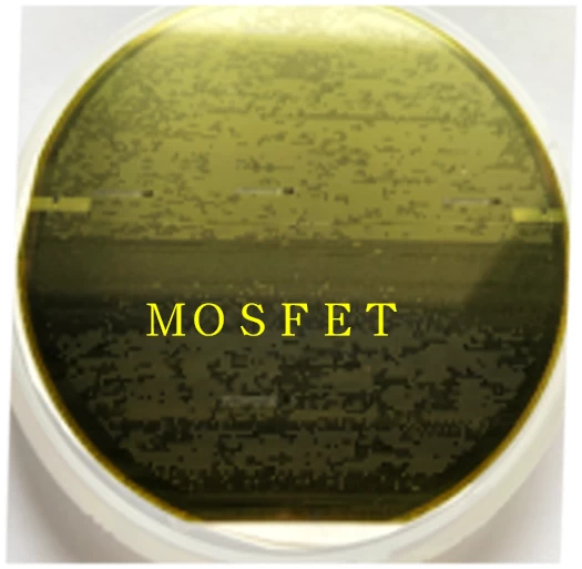
  • Automotive: SiC-based inverters, diodes, MOSFETs, and IGBTs.
  • Industrial Heating
  • Seals and Bearings

These attributes together contribute to elevated quality, efficiency,

Ceramic Micromachining

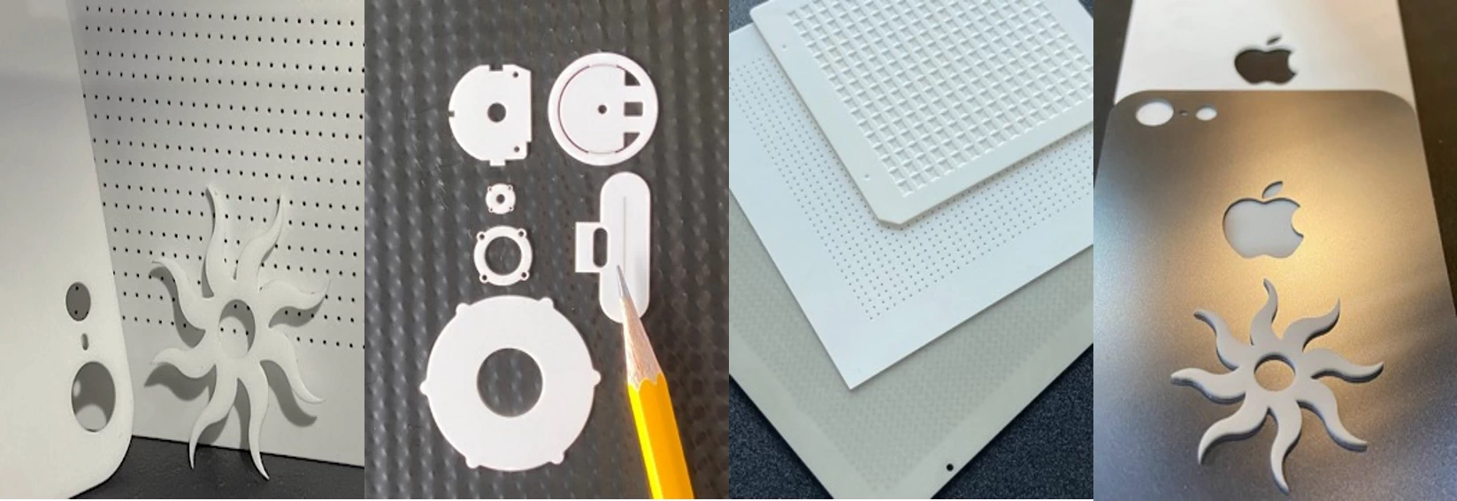
Laser micromachining finds applications in electronics ceramic substrates for various purposes, including creating micro-vias, microchannels, surface texturing, devices substrates, and modifying electrical properties.

If you’re using ceramic substrates for high-frequency communication devices and aren’t satisfied with the cost or performance, have you thought about switching to glass substrates? Feel free to get in touch with us – our TGV-related technology could provide a solution

IC Vertical Probe Card

Laser micromachining finds applications in electronics ceramic substrates for various purposes, including creating micro-vias, microchannels, surface texturing, devices substrates, and modifying electrical properties.

If you’re using ceramic substrates for high-frequency communication devices and aren’t satisfied with the cost or performance, have you thought about switching to glass substrates? Feel free to get in touch with us – our TGV-related technology could provide a solution

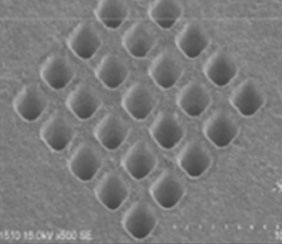
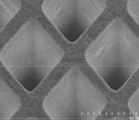
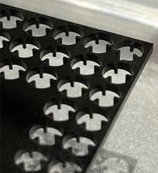
20x20 um High aspect ratio square hole drilling in the guide plate

Material: Si3N4
Guide Plate for vertical
Probe card

Square Hole: 30×30μm
Wall thickness: 5μm
Material thicjness 200μm

The image displays an authentic IC probe card guide plate with a hole array of 20,000 holes in a 10 mm square area.

Laser Wafer Dicing

Numerous cutting-edge silicon wafers feature intricate multi-layered structures, 3D designs, and delicate functional materials. Some are highly sensitive to water or particle contamination during dicing, while others possess non-standard chip shapes, making them incompatible with traditional diamond saws. Hi-Nano has pioneered diverse strategies to address these challenges, encompassing downsizing wafers, dicing MEMS wafers, handling Low-k wafers, and efficiently dicing glass-passivated wafers, among other techniques.

Diamond Laser Processing

Our laser systems are designed to efficiently handle CVD, PCD, PCBN, and MCD materials, encompassing tasks such as laser slicing, cutting, faceting, marking, and polishing.

Here are a few examples of items that have been machined using lasers :

Medical components made from CVD diamond.

Laser Slicing of CVD diamonds
( Before cleaning )

Creation of diamond windows.