Laser Micromachining Services

Hi-Nano specializes in delivering cutting-edge solutions for challenging high-precision machining needs across a wide range of materials. Our state-of-the-art technology and expert team are dedicated to providing exceptional results for our customers.

Materials Expertise & Applications

Explore our job shop’s diverse services covering various materials and applications, conveniently categorized. Contact us if you need assistance – we’re here to help with pleasure.

Optical Glass

Silicon & SiC

Ceramics

Diamonds

Lithium Niobate (LN)

Polymers and PI

Thin Metals

Advanced Materials

TGV / Glass Core

We offer customized TGV and Glass Core Job Shop Services

Through-Glass-Vias (TGV) technology involves creating microscopic vias through glass substrates, enabling intricate three-dimensional connections in microelectronic devices.
This breakthrough technology has found applications across various industries due to its unique advantages.

Functions:

  • High-Density Interconnections
  • Reduced signal losses
  • Improved Thermal Management

Major Markets:

  • Semiconductor Industry : Enabling advanced 2.5D and 3D packaging.
  • Telecommunications : TGV is crucial for high-performance components in telecommunications, supporting the demand for low-loss, faster and more reliable communication devices.
SP-01-1

Our Technology Features : Hole diameter: > 10um

  • Aspect ratio: 1:20
  • Straight side wall
  • No chipping and microcracks
  • High accuracy
SP-01-2

Versatility in Applications:

Our TGV technology is not just a solution; it's a versatile tool for various applications. From semiconductor packaging to medical devices and beyond, our TGV capabilities cater to a wide range of industries.

Custom Jobshop Services:

We provide custom jobshop services to meet the unique needs of our clients. Whether you require prototype development or large-scale production, our team is ready to deliver excellence.

Connect with Us:

Contact us today to experience how our innovative solutions and job shop services can propel you to success.

AR/VR/MR Lenses

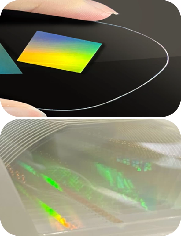
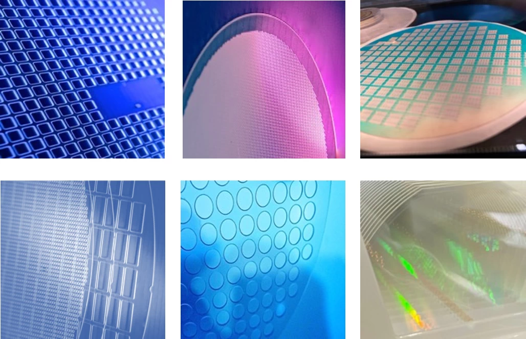
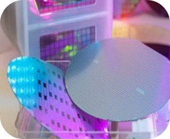
Given the presence of nanostructured optic devices on the wafer, a high-cleanliness environment is imperative. The entire process is meticulously executed within a Class 1000 cleanroom to ensure that all sensitive components remain uncontaminated, free from dust or any inadvertent contact.

Applications:

  • Capable of cutting both straight lines and free shapes with precision.
  • Accommodates a wide range of glass thicknesses, from ultra-thin and bendable to ultra-thick glass.
  • Enables cutting and drilling of various optical glass types with exceptional accuracy.
  • Delivers high cutting quality for coated lenses, ensuring superior results.
  • Cutting of AR/VR/MR lenses
  • Dicing of optical gratings
  • Dicing of optical waveguides
  • Dicing of MEMS Micro Lens Array
  • Dicing of Lidar optics
  • Dicing of high-precision optical encoders
  • Micro marking of Reticles lens.
  • Dicing of Meta Optical Elements
  • Dicing of Photo Mask

Glass Wafers

At Hi-Nano, we have the expertise to provide a wide range of glass wafers, each tailored to unique applications. Our offerings include glass spacers, glass carrier wafers, glass interposers, micro and nano-structured glass wafers, and glass capping wafers. We also supply TGV (Through Glass Vias) glass substrates, catering to the semiconductor industry and high-frequency telecommunications. These wafers are essential for advanced IC packages, enabling 2.5D and 3D packaging solutions. Trust Hi-Nano for your glass wafer needs, designed to meet the demands of cutting-edge technology

Application examples:

  1. Glass interposer, spacer and carrier wafers.
  2. Wafer-Level Packaging.
  3. Wafer-Level Optics.
  4. Micro & nano structured glass wafers.
  5. Photonic Integrated Circuits (PICs).
  6. Waveguides and splitters.
  7. Glass wafers for High-Frequency Devices substrate.
  8. Glass wafers for Lab-on-a-chip devices.
  9. AR/VR/ MR glass wafers.
  10. Glass wafer for MEMS based sensors.
  11. Glass wafer for RF filters.

These examples illustrate the versatility of glass wafers across a range of industries, from semiconductor manufacturing to medical diagnostics and consumer electronics. HI-Nano’s capabilities in providing various types of glass wafers support innovation and technology advancements in these fields.

General Optical Glass

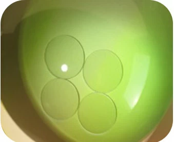
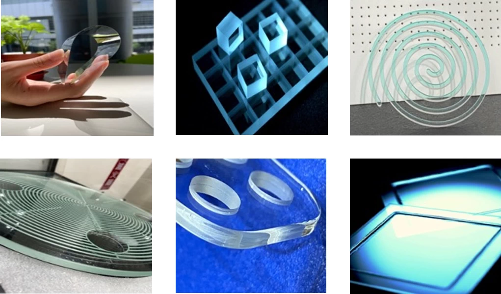
At HI-Nano, we harness the power of the latest laser technology to precision machine various types of optical glass. Our capabilities span the entire spectrum, from ultra-thin to ultra-thick glass, and from linear to freeform shapes. Our non-contact machining methods include cutting, hole drilling, grooving, selective thinning, glass inner marking, polishing, welding, and more. The beauty of our approach lies in its ability to deliver contamination-free results. This makes our services especially suited for critical applications in semiconductor, optics, medical, sensors, and military industries

Applications:

  • Ultra-thin ( 25um) glass cutting
  • Thick-glass (10mm)cutting
  • Spiral Glass cutting
  • 10 mm thick glass chuck
  • cutting and grooving
  • Glass joining and polishing
  • Capping bio-glass selective slimming.

Coated Glass

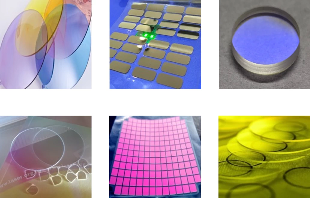
Dealing with coated glass, especially when it’s equipped with multilayers of materials, can be a challenging task. Traditional machining methods, whether mechanical or laser-based, often risk damaging the delicate coating layers. HI-Nano, however, has developed an innovative process that allows us to machine sensitive lenses without causing any damage to the lenses or sensors. This breakthrough technique is particularly beneficial for high-value optical lenses, sensors, and devices, ensuring the integrity of your coated glass products.

Applications:

  • Band-Pass Filters
  • Optical Sensors
  • Micro Lens Array
  • Lidar (Light Detection and Ranging)
  • Anti-Reflect Lens
  • Protective Windows
  • Dichroic Filters
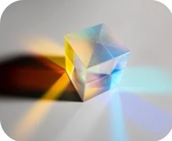
  • Beam Splitters
  • Polarizing Filters
  • Dielectric Mirrors
  • IR (Infrared) Windows
  • UV (Ultraviolet) Filters
  • Gradient Index (GRIN) Lenses
  • Sapphire Lenses
  • Diamond Lenses

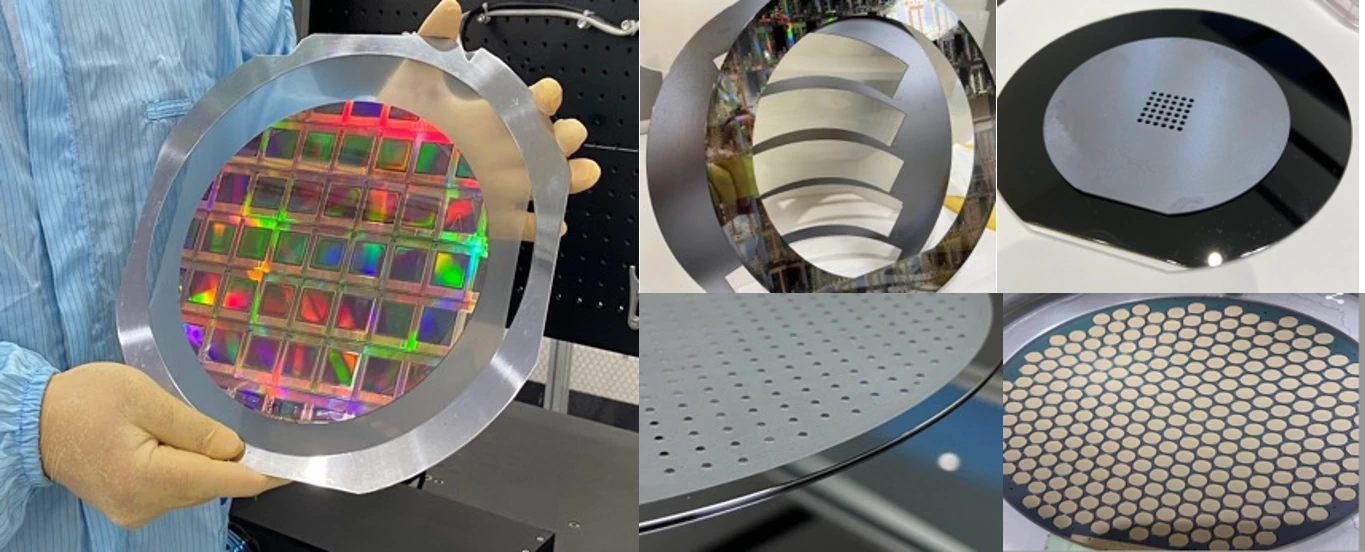
Precision Laser Micromachining for Silicon Wafer

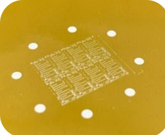
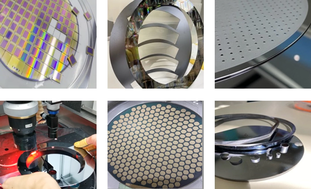
We excel in providing job shop services for Silicon wafers and SiC, addressing the challenges that conventional diamond saw machining methods often struggle to overcome.

Our commitment to precision and advanced technology ensures that we meet the specialized requirements of the semiconductor and electronics industries. Count on HI-Nano for your job shop services needs, and let us help you achieve remarkable results in silicon and SiC micromachining.

Applications:

  • Wafer downsizing
  • Low-k wafer dicing
  • Ultra-thin wafer dicing
  • Micro mirror array wafer dicing
  • MEMS wafer with moving parts
  • Nano structured optical wafers
  • Taiko ring wafer dicing
  • Muti-project wafer selective dicing
  • Gpp Round dice power devices dicing
  • Raised dots wafer machining

Laser machining for SiC ( Silicon Carbide )

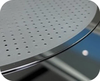
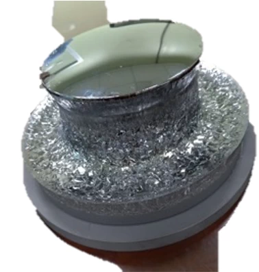
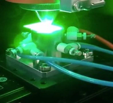
SiC, a key material for next-generation semiconductors, boasts hardness just below diamond, making it extremely challenging to machine. In response, Hi-Nano has pioneered laser machining solutions tailored for SiC  wafers, covering tasks like:

Ingot Slicing,  Freeform Dicing,  Hole Drilling,  Grooving,  Surface Texturing, and more.

Additionally, Hi-Nano excels in machining thick sintered SiC to create essential tools and machine parts for semiconductor manufacturing equipment, including precision components like SiC wafer chuck tables, focus rings, and wafer carriers.

Notably, Hi-Nano’s approach exclusively relies on laser non-contact processes, eliminating tool wear issues. This unique attribute makes it ideal for applications requiring the precise drilling of numerous tiny holes, such as in SiC shower heads.
Laser Micro Machining for Ceramics

Hi-Nano offers laser job shop services that specialize in a variety of high-performance ceramics widely utilized in semiconductor and microelectronics, energy, military, medical, and RF device applications. These ceramics include Green tape, LTCC, Zirconia, PZT, and advanced composite ceramics.

Our applications encompass:

  • Precise perforation and cutting of AlN and Al2O3 substrates.
  • High-precision hole drilling (30 x 40 microns) on Si3N4 (Silicon Nitride substrate) for IC probe cards.
  • Freeform cutting of Zirconia.
  • Laser cutting of PZT (Piezoelectric material).

Explore the precision and versatility of our Laser Micromachining services for your ceramic needs.

Laser Wafer Dicing

Numerous cutting-edge silicon wafers feature intricate multi-layered structures, 3D designs, and delicate functional materials. Some are highly sensitive to water or particle contamination during dicing, while others possess non-standard chip shapes, making them incompatible with traditional diamond saws. Hi-Nano has pioneered diverse strategies to address these challenges, encompassing downsizing wafers, dicing MEMS wafers, handling Low-k wafers, and efficiently dicing glass-passivated wafers, among other techniques.

Exemplary Precision in Laser Diamond Processing

Slicing, Slotting, Free Shape Cutting, Hole Drilling,  Milling

Our advanced techniques shape lab-grown diamonds into versatile tools and substrates for various applications. From Heat spreaders and IC substrates to engineering components for high-power and AI devices, our precision serves diverse industries, including semiconductor and high-frequency communications.

Immerse yourself in the excellence of each cut, where precision meets innovation at Hi-Nano.

  • We welcome both experimental projects and long-term contract job shop services. Connect with us today to leverage the latest advancements in laser technology for your benefit.

Lithium Niobate (LN)

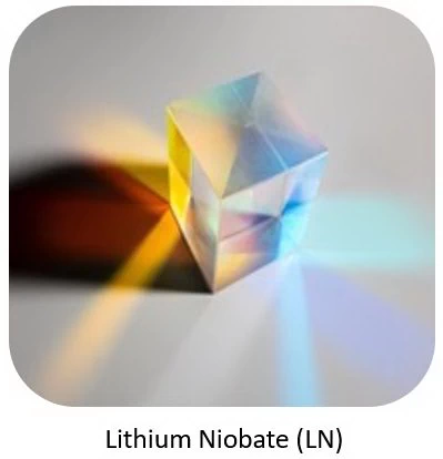
Lithium Niobate (LiNbO₃ or LN) is a highly versatile optical material, renowned for its broad transparency range and exceptional properties. Widely used in electro-optics, acoustic-optics, nonlinear optics, waveguides, and fiber optic gyroscopes (FOGs), LN offers high electro-optic and nonlinear optic coefficients, along with excellent electromechanical coupling and stability.

While LN wafers with different crystal orientations pose laser processing challenges, Hi-Nano has developed innovative solutions. For any laser processing difficulties with LN, contact us for tailored solutions to your specific needs.

Polymers and PI

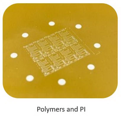
Hi-Nano uses versatile laser systems for precise processing of polyimide (PI) and similar flexible materials in microelectronics, FPCBs, RDL, and IC probe card isolation layers. These systems perform tasks like free-shape cutting and micro-hole drilling without heat-affected zones.

Laser processing typically follows electronic component mounting, often with other substrates. Polyimides, commonly in thin, flexible circuit boards, also serve in energy storage and alternative energy insulation.

Their exceptional properties, including resistance to extreme temperatures (-256° to 400°C), make them widely used in aerospace. Kapton films, a type of polyimide, can be laminated, metallized, or coated with adhesives.
Thin Metals

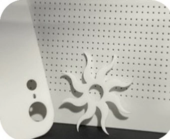
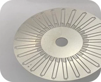
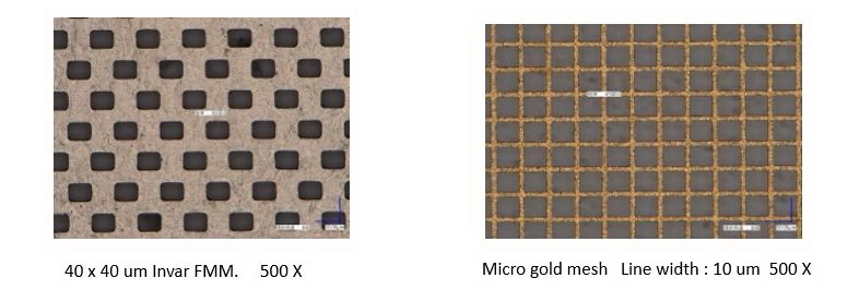
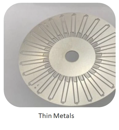
Hi-Nano showcases the capability to precisely process thin metal sheets and metal foil at the micron level, guaranteeing impeccable results free from debris, deformation, oxidation, or the formation of a Heat Affected Zone (HAZ).

This state-of-the-art technology is versatile, serving both in the production and repair of Fine Metal Masks (FMM) and other intricate thin metal components.

Feel free to reach out to us if you have any thin metal parts that require micromachining.

Demonstrations of Thin Metal Applications

Explore various applications across diverse fields enabled by our advanced thin metal laser micromachining technology. Examples include:

FMM (Fine Metal Mask) for OLED manufacturing
Precision stencils for screen printing
Production of micro probes for IC probing
Micro filters
Micro gold mesh for medical applications

Discover how our technology can be customized for a wide range of applications and industries.

Feel free to reach out to us if you have any thin metal parts that require micromachining.

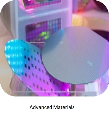
Advanced Materials

Recently, driven by the substantial market demand for artificial intelligence, the Internet of Things, and advancements in 5G, 6G, and LEO communications, a large amount of cutting-edge materials for optical, communication, and IC 3D packaging continues to emerge. This includes multi-layer composite functional materials, presenting challenges beyond the scope of conventional methods.

Hi-Nano has consistently assisted customers in addressing diverse specialized processing issues, accumulating extensive expertise in precision processing over the years.

Consequently, when faced with materials that are challenging to machine, Hi-Nano may already have effective solutions.

Simply reach out to Hi-Nano  –  your challenging issues might find a resolution.
Showcase

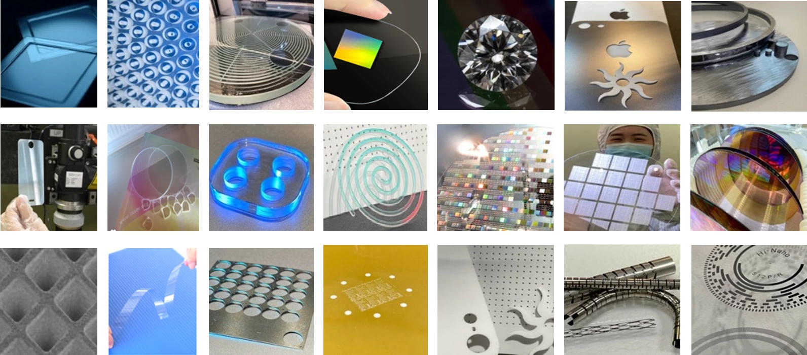
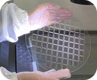
The showcased examples demonstrate our job shop services, featuring a wide range of materials and versatile micro-machining skills for diverse tasks.

Hi-Nano provides end-to-end job shop services, from R&D to mass production, delivering high-quality solutions that accelerate our customers’ success with efficiency and cost-effectiveness.