Laser Micromachining Services
Applications:
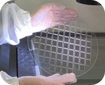
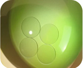
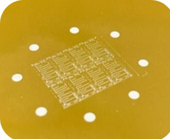
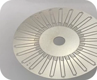
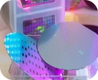
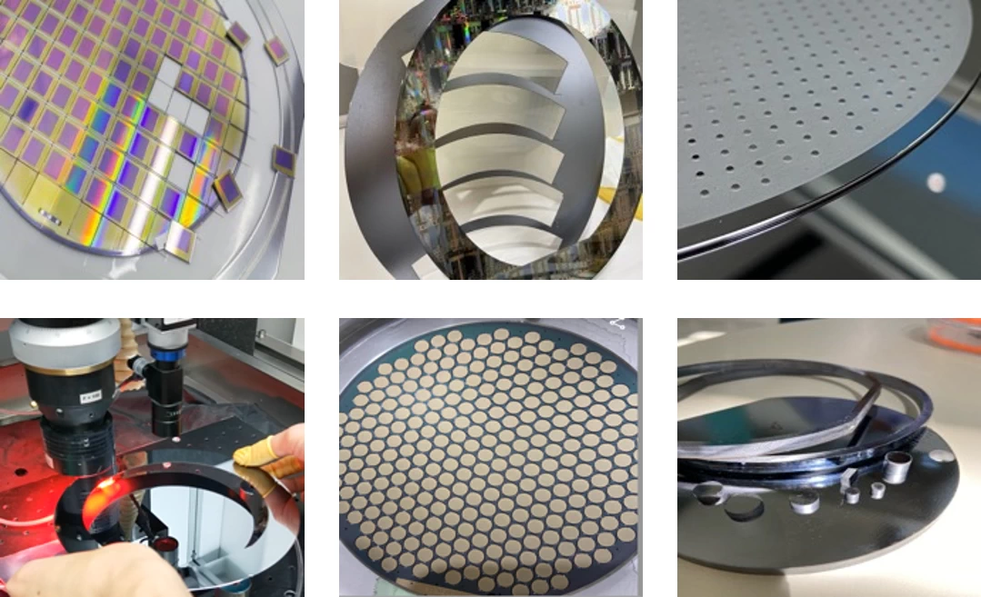
- Wafer downsizing
- Low-k wafer dicing
- Ultra-thin wafer dicing
- Micro mirror array wafer dicing
- MEMS wafer with moving parts
- Nano structured optical wafers
- Taiko ring wafer dicing
- Muti-project wafer selective dicing
- Gpp Round dice power devices dicing
- Raised dots wafer machining
Laser machining for SiC ( Silicon Carbide )
SiC, a key material for next-generation semiconductors, boasts hardness just below diamond, making it extremely challenging to machine. In response, Hi-Nano has pioneered laser machining solutions tailored for SiC wafers, covering tasks like:
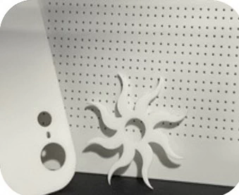
Ingot Slicing, Freeform Dicing, Hole Drilling, Grooving, Surface Texturing, and more.
Additionally, Hi-Nano excels in machining thick sintered SiC to create essential tools and machine parts for semiconductor manufacturing equipment, including precision components like SiC wafer chuck tables, focus rings, and wafer carriers.
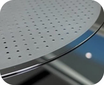
Notably, Hi-Nano’s approach exclusively relies on laser non-contact processes, eliminating tool wear issues. This unique attribute makes it ideal for applications requiring the precise drilling of numerous tiny holes, such as in SiC shower heads.
